
Electron microscopes
Electron microscopy uses an electron beam to create an image of a sample. Because of this an electron microscope has a much greater resolving power than a light microscope and is capable of much highermagnifications (up to 2 million times). There are two types of electron microscopes - transmission electron microscopes (TEM) and scanning electron microscopes (SEM).

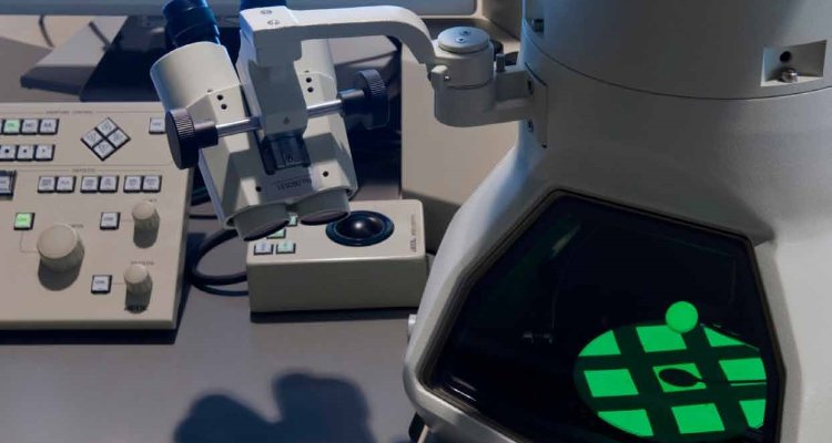
JEOL JEM-1400Plus
The JEM-1400Plus features high resolution/high contrast imaging, outstanding TEM analytical performance, cryomicroscopy, 3D tomography, and montaging. This compact, easy-to-use TEM is suitable for biological, polymer, and materials science applications. JEOL JEM-1400Plus has an acceleration voltage up to 120kV. The machine accommodates measurements under cryogenic temperatures, using the available cryo-holder and sample preparation equipment for imaging thin biological and other aqueous samples.
Specifications
- High resolution 120 kV transmission electron microscope
- High-sensitivity sCMOS, "Matataki Flash" Camera
- Ultra-wide area montage system, Limitless Panoram (LLP)
- High-tilt specimen holder (tilting from -70° to 70°) for tomography
- Software for automated recording of tilt series
- JEOL TEMographyTM suite (Recorder, Composer and Visualizer)
- SerialEM, Chimera, Image J
- GATAN cryo-holder

FIB-SEM Zeiss Auriga (Crossbeam)
The Zeiss Auriga is a high resolution Focused Ion Beam Scanning Electron microscope. The Schottky field emitter allows a resolution downto 1 nm of the full 30 to 1 kilovolt range. The microscope has Inlens, Everhart-Thornley and backscatter detectors. Furthermore the microscope is equipped with a Gatan Alto 2500 cryo-stage, cryo-transfer and coating system. The EDS system is from Oxford Instruments for Energy Dispersive X-ray Spectroscopy. The Focused Ion Beam can directly modify or "mill" a sample surface with nanometer precision. The focused ion beam is used to etch the sample, thereby exposing a new surface which van be imaged by SEM. Repeating this process can reveal the full 3D representation of the internal structure.Specifications
- Ultra high-resolution field emission scanning electron microscope
- Schottky Field Emitter
- Focused Ion Beam (Ga Liquid metal ion source
- SIngle Gas Injection System (GIS) platimu precursor
- Charge Compenstation
- Inlens, SE (Everhardt-Thornley) and Esb (Energy and Angle Selective) detection
- SmartSEM user interface
- Gatan Alto2500 cryotransfer (/coating) system
- EDX Oxford 80 mm detector - Aztec user interface
- Resolution downto 1-2 nm (a6 30-1 kV, Ga FIB resolution ~ 3nm

FEI Magellan 400 FESEM
The Magellan 400 is a fully digital FESEM with Schottkey field emitter source providing subnanometer resolution over the full 1 kV to 30 kV electron energy range. The microscope has two detectors a Everhart-Thornley SE detector for SE detection, and NG in-lens detector (TLD) designed for high-resolution imaging even at low kV’s. The Magellan is equipped with a new generation energy dispersive spectroscopy (EDS) system from Oxford Instruments. Furthermore the Magellan is equipped with a cryostage and cryotransfer system.
Specifications
- High resolution scanning electron microscope
- Accelerating Voltage: 50V-30kV
- Beam current: 0.6 pA to 22 nA
- Resolution: 0.8nm@15kV, 0.9nm@1kV
- Leica VCT100 cryotransfer system
- Leica cryoMED020 cryopreparation unit
- Oxford Aztec EDX
- “Under” lens SE and BSE detection